Printed Circuit Board Assembly Manufacturer

All Categories

Get a Free Quote

Our representative will contact you soon.
Email
Phone
WhatsApp
Name
Message
0/1000
Upload File
Please upload at least an attachment
Up to 3 files, each no larger than 30MB. Supported formats: jpg, jpeg, png, pdf, doc, docx, xls, xlsx, csv, txt, stp, step, igs, x_t, dxf, prt, sldprt, sat, rar, zip.

Printed circuit board assembly manufacturer

Printed circuit board assembly (PCBA) is a critical process in the manufacturing of electronic devices, facilitating the connection of electronic components on a printed circuit board (PCB). As a printed circuit board assembly manufacturer, Suntech Electronics specializes in providing reliable, high-quality PCB and PCBA solutions for various industries including aerospace, medical, and automotive. This article will explore key specifications, through hole pcb assembly service methods, installation guidance, common issues, and the advantages of High-Density Interconnect (HDI) technology, all of which are essential for B2B buyers evaluating PCB assembly services.
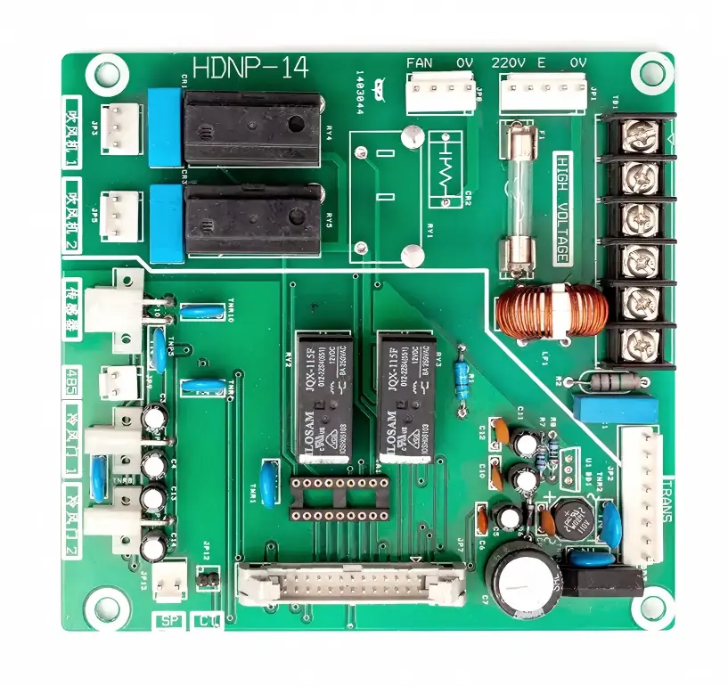
Key Specifications for High-Quality PCB Assembly Projects

When considering a PCB assembly project, several specifications must be taken into account to ensure optimal performance. Key specifications include: 

Layer Count: PCBs can range from simple single-layer designs to complex multi-layer configurations (up to 50 layers). The layer count affects the board's complexity and functionality. Buyers must assess their application requirements to determine the appropriate layer count. 

Material Selection: The choice of substrate material, such as FR-4, Rogers, or aluminum, impacts thermal performance, electrical insulation, and mechanical stability. Each material has its unique properties, making it essential to select the right one based on the application's specific needs. 

Surface Finish: The surface finish, such as HASL, ENIG, or OSP, is crucial for solderability and long-term reliability. Different finishes are suitable for various applications, and buyers should confirm their compatibility with the components being used. 

Trace Width and Spacing: The width of the traces and the spacing between them determine the current-carrying capacity and overall space efficiency. This is particularly important in high-density applications where space is constrained. 

Testing Requirements: It’s vital to define testing standards upfront, including In-Circuit Testing (ICT), X-ray inspection, and other quality assurance measures to ensure the pcb box build assembly services meets performance criteria. 

By thoroughly understanding these specifications, buyers can collaborate effectively with their PCB assembly manufacturer to achieve the desired results.

Get a Free Quote

Our representative will contact you soon.
Email
Phone
WhatsApp
Name
Message
0/1000
Upload File
Please upload at least an attachment
Up to 3 files, each no larger than 30MB. Supported formats: jpg, jpeg, png, pdf, doc, docx, xls, xlsx, csv, txt, stp, step, igs, x_t, dxf, prt, sldprt, sat, rar, zip.

Related product categories

SMT vs. DIP Assembly

SMT vs. DIP Assembly

Surface Mount Technology (SMT) and Dual In-line Package (DIP) assembly are two common methods of PCB assembly, each with its advantages and applications. 

SMT Assembly: SMT involves mounting components directly onto the surface of the PCB. This method allows for a higher component density and reduced overall size, making it ideal for compact electronic devices. SMT components are typically smaller and lighter, which can lead to improved performance and efficiency. However, SMT requires precise placement and soldering techniques, often involving automated processes like pick-and-place machines. 

DIP Assembly: DIP assembly, on the other hand, involves inserting component leads through holes in the PCB and soldering them on the opposite side. While this method is generally easier and cheaper for prototyping due to its manual handling, it is less suitable for high-density applications where space is at a premium. DIP components typically consume more board space and may not provide the same level of performance as SMT components. 

Choosing between SMT and DIP depends on the project requirements, including component availability, through hole assembly services cost, and space constraints. Suntech Electronics can assist buyers in selecting the most suitable method for their specific application.
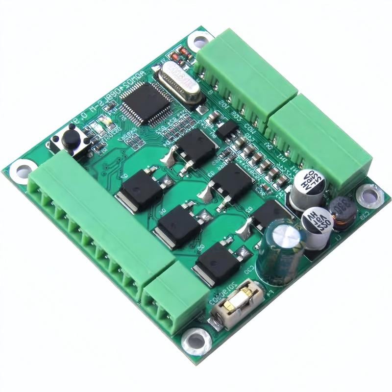
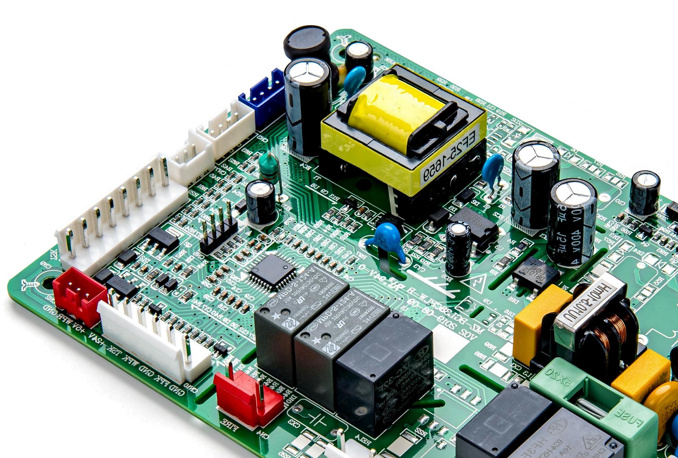
Installation Guidance for Effective PCB Assembly Applications

Installation Guidance for Effective PCB Assembly Applications

Proper installation is critical for the functionality and longevity of PCB assemblies. Below are some key considerations for effective installation: 

Pre-Assembly Inspection: Before installation, a thorough inspection of the PCB should be conducted to ensure that there are no physical defects, such as scratches or misalignments, that could impair performance. 

Controlled Environment: PCB assemblies should be installed in a controlled environment to prevent contamination from dust, moisture, or static electricity. Utilizing anti-static mats and wrist straps can help mitigate electrostatic discharge (ESD) risks. 

Component Orientation and Placement: Ensuring correct orientation during installation is crucial. Misalignment can lead to shorts or open circuits. Proper labeling and alignment guides can aid in this process. 

Soldering Techniques: When soldering, it’s important to use the appropriate temperature and technique to avoid damaging components. For SMT, reflow soldering is standard, while DIP components typically require wave soldering. 

Final Testing: After installation, conduct functional testing to verify that the assembly operates as intended. This may include ICT and in-field testing under actual operating conditions. 

Following these guidelines can help ensure that PCB assemblies perform reliably in their intended applications.

Common Problems in PCB Assembly and Their Practical Solutions

Common Problems in PCB Assembly and Their Practical Solutions

Despite careful planning, several common issues can arise during PCB assembly. Understanding these issues and their solutions can help buyers avoid costly mistakes: 

Soldering Defects: Common soldering issues include cold solder joints, solder bridges, and insufficient solder. To mitigate these problems, ensure proper temperature control and use high-quality solder paste. Implementing automated soldering techniques can also enhance consistency. 

Component Placement Errors: Misalignment during the assembly process can lead to functional failures. Regular calibration of placement machines and thorough pre-assembly checks can help minimize these errors. 

Material Compatibility: Using incompatible materials can result in delamination or thermal stress. Buyers should confirm compatibility between the PCB materials and the components being used, especially in high-stress environments. 

Environmental Factors: Exposure to moisture, dust, or extreme temperatures during assembly can adversely affect performance. Implementing a controlled environment for assembly can significantly reduce these risks. 

Testing Failures: If assemblies fail testing, it’s important to conduct a root cause analysis to identify the source of the issue. Continuous improvement practices, such as regular training for assembly personnel, can enhance overall quality and reduce defects. 

By being aware of these common problems and their solutions, buyers can work closely with their PCB assembly manufacturer to ensure a smooth production process.

Benefits of High-Density Interconnect (HDI) in PCB Design

High-Density Interconnect (HDI) technology offers significant advantages in PCB design, making it an increasingly popular choice for modern electronic applications: 

Space Efficiency: HDI PCBs allow for smaller and lighter designs due to their fine pitch and microvias, which enable higher routing density. This is particularly beneficial in compact devices where space is limited. 

Improved Performance: HDI technology enables shorter interconnections, which can reduce signal distortion and electromagnetic interference. This leads to enhanced overall performance and reliability, especially in high-speed applications. 

Cost-Effective Solutions: While HDI PCBs may have higher initial manufacturing costs, their efficiency can lead to reduced material and assembly costs in the long run. The ability to accommodate more components in a smaller space can also lower overall project costs. 

Enhanced Thermal Management: HDI designs often incorporate advanced thermal management techniques, which can help dissipate heat more effectively in high-performance applications. 

Flexibility in Design: HDI technology supports a variety of designs and configurations, allowing for greater customization to meet specific application requirements. 

Understanding the benefits of HDI technology can help buyers make informed decisions when selecting PCB assembly services, particularly for advanced electronic applications. Suntech Electronics is equipped to provide expert guidance and solutions tailored to meet the unique demands of HDI PCB designs. 

Get a Free Quote

Our representative will contact you soon.
Email
Phone
WhatsApp
Name
Message
0/1000
Upload File
Please upload at least an attachment
Up to 3 files, each no larger than 30MB. Supported formats: jpg, jpeg, png, pdf, doc, docx, xls, xlsx, csv, txt, stp, step, igs, x_t, dxf, prt, sldprt, sat, rar, zip.